Power transistors are one of the main contributors to power loss in switching power supplies. Transistor losses are generally divided into two categories; conduction losses and switching losses. Conduction losses are the losses incurred when a transistor conducts current, while switching losses are the losses that occur when transitioning between switching states.
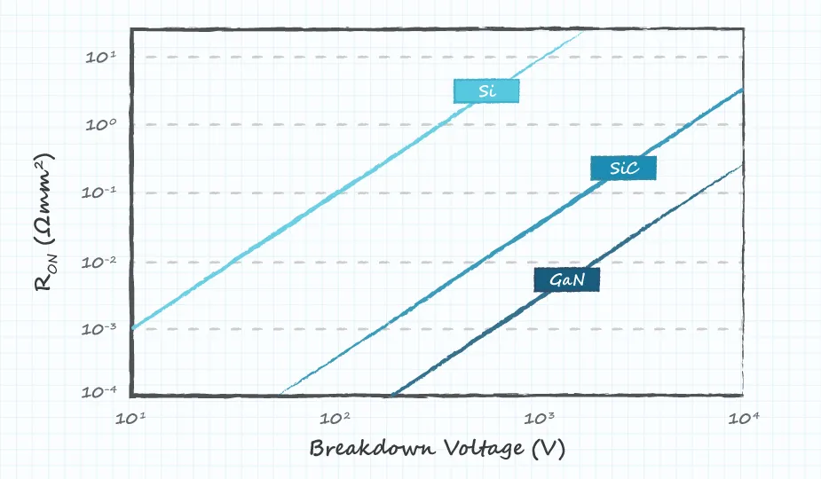
When turned on, a GaN transistor (like a silicon transistor) acts like a resistor between drain and source, usually denoted Ron, and conduction losses are proportional to this resistance. The main advantage of GaN and other WBG materials is their relationship between breakdown voltage and Ron. Figure 1 shows the theoretical limits of this relationship for silicon, GaN and silicon carbide (SiC, another WBG material). It can be seen that when a given breakdown voltage is reached, the Ron of WBG devices is much lower than that of silicon, and GaN is the lowest among the three. As silicon is approaching its theoretical limit, continuing to increase Ron will require the use of GaN and other WBG materials.

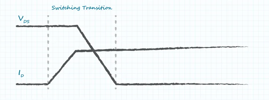
In addition to improving conduction losses, using GaN also reduces switching losses. Several factors contribute to switching losses, several of which can be improved by using GaN. One loss mechanism is due to the current flowing in the transistor before the drain-source voltage starts to drop, as shown in Figure 2. During this period, the losses (equal to the product of voltage and current) are very large. Increasing the speed at which the switch turns on will reduce the losses incurred during transitions. GaN transistors can be turned on faster than silicon transistors, so losses from this switching are reduced.

Another way GaN reduces switching losses is by not using body diodes. To avoid a short circuit condition, there is a period of time when both switches of the half bridge are open, called the "dead time". During this time, current continues to flow, but since both switches are closed, current is forced through the body diode. The efficiency of the body diode when turned on is much lower than the Ron resistance of a silicon transistor. GaN transistors do not have body diodes. The current flowing through the body diode of the silicon transistor instead flows through the Ron resistor. This significantly reduces losses incurred during dead time.
Since the body diode of a silicon transistor conducts during the dead time, it must be turned off when another switch is turned on. During this time, current flows in the reverse direction after the diode turns off, increasing losses. There is no body diode in GaN transistors, so reverse recovery losses are close to zero.